Multiple Choice Questions Topic Outline
- MCQs in Field-Effect Transistors (FETs)
- MCQs in JFET
- MCQs in JFET Characteristics and Parameters
- MCQs in JFET Biasing
- MCQs in The Ohmic Region
- MCQs in MOSFET
- MCQs in MOSFET Characteristics and Parameters
- MCQs in MOSFET Biasing
- MCQs in IGBT
Begin and Good luck!
1. On the drain characteristic curve of a JFET for VGS = 0, the pinch-off voltage is
- A) below the ohmic area.
- B) between the ohmic area and the constant current area.
- C) between the constant current area and the breakdown region.
- D) above the breakdown region.
2. For a JFET, the value of VDS at which ID becomes essentially constant is the
- A) pinch-off voltage.
- B) cutoff voltage.
- C) breakdown voltage.
- D) ohmic voltage.
3. The value of VGS that makes ID approximately zero is the
- A) pinch-off voltage.
- B) cutoff voltage.
- C) breakdown voltage.
- D) ohmic voltage.
4. For a JFET, the change in drain current for a given change in gate-to-source voltage, with the drain-to-source voltage constant, is
- A) breakdown.
- B) reverse transconductance.
- C) forward transconductance.
- D) self-biasing.
5. High input resistance for a JFET is due to
- A) a metal oxide layer.
- B) a large input resistor to the device.
- C) an intrinsic layer.
- D) the gate-source junction being reverse-biased.
6. A dual-gated MOSFET is
- A) a depletion MOSFET.
- B) an enhancement MOSFET.
- C) a VMOSFET.
- D) either a depletion or an enhancement MOSFET.
7. Which of the following devices has the highest input resistance?
- A) diode
- B) JFET
- C) MOSFET
- D) bipolar junction transistor
8. A self-biased n-channel JFET has a VD = 6 V. VGS = –3 V. Find the value of VDS.
- A) –3 V
- B) –6 V
- C) 3 V
- D) 6 V
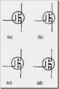
9. Refer to Figure 8-1. Identify the p-channel E-MOSFET.
Figure 8-1
- A) a
- B) b
- C) c
- D) d
10. Refer to Figure 8-1. Identify the n-channel D-MOSFET.
- A) a
- B) b
- C) c
- D) d
11. Refer to Figure 8-1. Identify the n-channel E-MOSFET.
- A) a
- B) b
- C) c
- D) d
12. Refer to Figure 8-1. Identify the p-channel D-MOSFET.
- A) a
- B) b
- C) c
- D) d
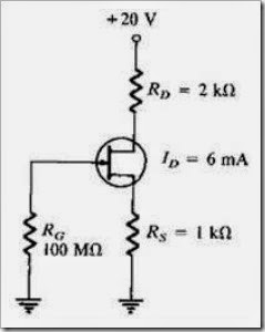
13. Refer to Figure 8-2(a). ID = 6 mA. Calculate the value of VDS.
Figure 8-2
- A) –6 V
- B) 6 V
- C) 12 V
- D) –3 V
14. Refer to Figure 8-2(b). ID = 6 mA. Calculate the value of VDS.
- A) 13.2 V
- B) 10 V
- C) 6.8 V
- D) 0 V
15. Refer to Figure 8-2(c). ID = 6 mA. Calculate the value of VDS.
- A) –9 V
- B) 9 V
- C) 6 V
- D) –3 V
16. A JFET data sheet specifies VGS(off) = –6 V and IDSS = 8 mA. Find the value of ID when VGS = –3 V.
- A) 2 mA
- B) 4 mA
- C) 8 mA
- D) none of the above
17. A JFET data sheet specifies VGS(off) = –10 V and IDSS = 8 mA. Find the value of ID when VGS = –3 V.
- A) 2 mA
- B) 1.4 mA
- C) 4.8 mA
- D) 3.92 mA
18. Refer to Figure 8-3. Determine the value of VS.
Figure 8-3
- A) 20 V
- B) 8 V
- C) 6 V
- D) 2 V
19. Refer to Figure 8-3. Calculate the value of VD.
- A) 20 V
- B) 8 V
- C) 6 V
- D) 2 V
20. Refer to Figure 8-3. What is the value of IG?
- A) 6 mA
- B) 4 mA
- C) 2 mA
- D) 0 mA
21. Refer to Figure 8-3. Determine the value of VGS.
- A) –20 V
- B) –8 V
- C) –6 V
- D) –2 V
22. Refer to Figure 8-3. Calculate the value of VDS.
- A) 0 V
- B) 2 V
- C) 4 V
- D) –2 V
23. The JFET is always operated with the gate-source pn junction _____ -biased.
- A) forward
- B) reverse
24. What three areas are the drain characteristics of a JFET (VGS = 0) divided into?
- A) ohmic, constant-current, breakdown
- B) pinch-off, constant-current, avalanche
- C) ohmic, constant-voltage, breakdown
25. What type(s) of gate-to-source voltage(s) can a depletion MOSFET (D-MOSFET) operate with?
- A) zero
- B) positive
- C) negative
- D) any of the above
26. The _____ has a physical channel between the drain and source.
- A) D-MOSFET
- B) E-MOSFET
- C) V-MOSFET
27. All MOSFETs are subject to damage from electrostatic discharge (ESD).
- A) true
- B) false
28. Midpoint bias for a D-MOSFET is ID = _____, obtained by setting VGS = 0.
- A) IDSS / 2
- B) IDSS / 3.4
- C) IDSS
29. In a self-biased JFET circuit, if VD = VDD then ID = _____.
- A) 0
- B) cannot be determined from information above
30. If VD is less than expected (normal) for a self-biased JFET circuit, then it could be caused by a(n)
- A) open RG.
- B) open gate lead.
- C) FET internally open at gate.
- D) all of the above
31. The resistance of a JFET biased in the ohmic region is controlled by
- A) VD.
- B) VGS.
- C) VS.
- D) VDS.


Nice quiz for newbies i learned about fet basics in this article
ReplyDelete