Visit: The New Homepage

Visit: The New Homepage
Kindly click the image for the updated Notes Online

Thursday, April 17, 2014

Subject: Transmission Media and Antenna Systems

0 comments Posted by Unknown at 10:08 PM
Hits:
Transmission Media and Antenna Systems Lecture

Course Name

  • TRANSMISSION MEDIA AND ANTENNA SYSTEMS

Course Description

  • Transmission media; radiowave propagation wire and cable transmission systems; fiber-optic transmission system; transmission lines and antenna systems.

Prerequisites:

  • Digital Communications
  • Electromagnetics

Course Objectives

Upon completion of the course, the student must be able to conceptualize,analyze and design transmission lines and antenna systems.
  • 1. Describe the types of transmission lines and calculate the line constants.
  • 2. Differentiate the types of radio wave propagation and be familiar with their applications.
  • 3. Understand the principle and characteristics of antennas , the different types as well as the methodology in the design of each.
  • 4. Be able to design and construct a wideband antenna ( VHF and UHF).

Transmission Media and Antenna Systems Outline

Following is the list of topics we will discuss in this course:
Transmission Media and Antenna Systems
Note: ADDING LESSON ON-PROGRESS . . .
LESSON 1: ON-PROGRESS . . .

Suggested References


credit: CMO 24 s2008©2013 www.FroydWess.com

Subject: Feedback and Control Systems

0 comments Posted by Unknown at 9:40 PM
Hits:
 Feedback and Control Systems Lecture

Course Name

  • FEEDBACK AND CONTROL SYSTEMS

Course Description

  • This course deals with time and frequency response of feedback control systems. The topics covered include, time response of first order and second order systems, modeling, transfer functions, pole-zero map, stability analysis, root locus, bode plots, compensators, PID controllers, and introduction to state-space techniques.

Prerequisites:

  • Advanced Engineering Mathematics

Course Objectives

Upon completion of the course, the student must be able to:

  • 1. Familiar with various systems exhibiting control mechanisms and understand their operation.
  • 2. Able to develop the value of being analytic and able to apply learned concepts to improve systems.
  • 3. Able to understand and appreciate feedback control.
  • 4. Able to apply system-level thinking
  • 5. Able to demonstrate knowledge of concepts in dealing with feedback and control systems

Feedback and Control Systems Outline

Following is the list of topics we will discuss in this course:

Feedback and Control Systems
Note: ADDING LESSON ON-PROGRESS . . .
LESSON 1: ON-PROGRESS . . .

Suggested References


credit: CMO 24 s2008©2013 www.FroydWess.com

Subject: Signals Spectra, and Signal Processing

0 comments Posted by Unknown at 9:17 PM
Hits:
Signals Spectra, and Signal Processing Lecture

Course Name

  • SIGNALS SPECTRA, AND SIGNAL PROCESSING

Course Description

  • Fourier transform; z transform; convolution; FIR filters; IIR filters; random signal analysis; correlation functions; DFT; FFT; spectral analysis; applications of signal processing to speech, image, etc.

Prerequisites:

Course Objectives

Upon completion of the course, the student must be able to conceptualize, analyze and design signals, spectra and signal processing system.

Signals Spectra, and Signal Processing Course Outline

Following is the list of topics we will discuss in this course:

Signals Spectra, and Signal Processing
Note: ADDING LESSON ON-PROGRESS . . .
LESSON 1: ON-PROGRESS . . .

Suggested References


credit: CMO 24 s2008©2013 www.FroydWess.com

Subject: Principles of Communications

0 comments Posted by Unknown at 8:59 PM
Hits:
Principles of Communications Lecture

Course Name

  • PRINCIPLES OF COMMUNICATIONS

Course Description

  • Bandwidth; filters; linear modulation; angle modulation; phase locked loop; pulse modulation; multiplexing techniques; noise analysis; radio transmitters and receivers.

Prerequisites:

Course Objectives

Upon completion of the course, the student must be able to:

  • 1. Conceptualize and analyze a communication system.
  • 2. design communication circuits and subsystems

Principles of Communications Course Outline

Following is the list of topics we will discuss in this course:

Principles of Communications
Note: ADDING LESSON ON-PROGRESS . . .
LESSON 1: ON-PROGRESS . . .

Suggested References


credit: CMO 24 s2008©2013 www.FroydWess.com

Subject: Energy Conversion

0 comments Posted by Unknown at 3:20 PM
Hits:
Energy Conversion Lecture

Course Name

  • ENERGY CONVERSION

Course Description

  • Principles of energy conversion and transducers: electromechanical, photoelectric, photovoltaic, thermoelectric, piezzoelectric; hall effect; reed switch; electrochemical, etc; generators, transformers; dynamic analysis, and fuel cells.

Prerequisites:

Course Objectives

The objective of the course is to introduce the concepts of energy conversion using transducers and be able to familiarize the students with the several applications of these devices.

Energy Conversion Course Outline

Following is the list of topics we will discuss in this course:

Energy Conversion
Note: ADDING LESSON ON-PROGRESS . . .
LESSON 1: ON-PROGRESS . . .

Suggested References


credit: CMO 24 s2008©2013 www.FroydWess.com

Subject: Electronic Devices and Circuits

0 comments Posted by Unknown at 2:48 PM
Hits:
Electronic Devices and Circuits Lecture

Course Name

  • ELECTRONIC DEVICES AND CIRCUITS / ELECTRONICS 1

Course Description

  • Introduction to quantum mechanics of solid state electronics; diode and transistor characteristics and models (BJT and FET); diode circuit analysis and applications; transistor biasing; small signal analysis; large signal analysis; transistor amplifiers; Boolean logic; transistor switch.

Prerequisites:

Course Objectives

Upon completion of the course, the student must be able to:

  • 1. Acquire a strong foundation on semiconductor physics; diode and diode circuit analysis; MOS and BJT (small and large signal) circuit analysis.
  • 2. Orientation: Review of Course
  • 3. Assessment of the Different Types of Learners
  • 4. Fundamentals of tubes and other devices
  • 5. Introduction of Semiconductors
  • 6. Diode Equivalent Circuits
  • 7. Wave Shaping Circuits
  • 8. Special Diode Application
  • 9. Power Supply And Voltage Regulation
  • 10. Bipolar Junction Transistor
  • 11. Small- Signal Analysis (BJT)
  • 12. Field Effect Transistor
  • 13. Small-Signal Analysis (FET)
  • 14. Large-Signal Analysis

Electronic Devices and Circuits Course Outline

Following is the list of topics we will discuss in this course:

Electronic Devices and Circuits
Note: ADDING LESSON ON-PROGRESS . . .
LESSON 1: ON-PROGRESS . . .

Suggested References

Robert L. Boylestad, Thomas L. Floyd
credit: CMO 24 s2008©2013 www.FroydWess.com

Monday, April 14, 2014

Field-Effect Transistors (FETs) - MCQs Answers

2 comments Posted by Unknown at 11:59 AM
Hits:
Answers key for  Field-Effect Transistors (FETs)
Below are the answers key for the Multiple Choice Questions (Quiz) in Field-Effect Transistors (FETs) .

1. between the ohmic area and the constant current area

2. pinch-off voltage

3. cutoff voltage

4. forward transconductance

5. the gate-source junction being reverse-biased

6. either a depletion or an enhancement MOSFET

7. MOSFET

8. 3 V

9. d

10. a

11. c

12. b

13. 6 V

14. 6.8 V

15. –9 V

16. 2 mA

17. 3.92 mA

18. 6 V

19. 8 V

20. 0 mA

21. –6 V

22. 2 V

23. reverse

24. ohmic, constant-current, breakdown

25. any of the above

26. D-MOSFET

27. true

28. IDSS

29. 0

30. all of the above

31. VGS

Back to Homepage


credit: Thomas L. Floyd©2013 www.FroydWess.com

Field-Effect Transistors (FETs) - MCQs

1 comments Posted by Unknown at 11:55 AM
Hits:
MCQs for  Field-Effect Transistors (FETs)

Multiple Choice Questions Topic Outline

  • MCQs in Field-Effect Transistors (FETs)
  • MCQs in JFET
  • MCQs in JFET Characteristics and Parameters
  • MCQs in JFET Biasing
  • MCQs in The Ohmic Region
  • MCQs in MOSFET
  • MCQs in MOSFET Characteristics and Parameters
  • MCQs in MOSFET Biasing
  • MCQs in IGBT

Begin and Good luck!

1. On the drain characteristic curve of a JFET for VGS = 0, the pinch-off voltage is

  • A) below the ohmic area.
  • B) between the ohmic area and the constant current area.
  • C) between the constant current area and the breakdown region.
  • D) above the breakdown region.

2. For a JFET, the value of VDS at which ID becomes essentially constant is the

  • A) pinch-off voltage.
  • B) cutoff voltage.
  • C) breakdown voltage.
  • D) ohmic voltage.

3. The value of VGS that makes ID approximately zero is the

  • A) pinch-off voltage.
  • B) cutoff voltage.
  • C) breakdown voltage.
  • D) ohmic voltage.

4. For a JFET, the change in drain current for a given change in gate-to-source voltage, with the drain-to-source voltage constant, is

  • A) breakdown.
  • B) reverse transconductance.
  • C) forward transconductance.
  • D) self-biasing.

5. High input resistance for a JFET is due to

  • A) a metal oxide layer.
  • B) a large input resistor to the device.
  • C) an intrinsic layer.
  • D) the gate-source junction being reverse-biased.

6. A dual-gated MOSFET is

  • A) a depletion MOSFET.
  • B) an enhancement MOSFET.
  • C) a VMOSFET.
  • D) either a depletion or an enhancement MOSFET.

7. Which of the following devices has the highest input resistance?

  • A) diode
  • B) JFET
  • C) MOSFET
  • D) bipolar junction transistor

8. A self-biased n-channel JFET has a VD = 6 V. VGS = –3 V. Find the value of VDS.

  • A) –3 V
  • B) –6 V
  • C) 3 V
  • D) 6 V

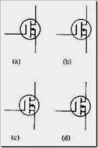
9. Refer to Figure 8-1. Identify the p-channel E-MOSFET.

MCQs in  Field-Effect Transistors (FETs) Fig. 01

Figure 8-1

  • A) a
  • B) b
  • C) c
  • D) d

10. Refer to Figure 8-1. Identify the n-channel D-MOSFET.

  • A) a
  • B) b
  • C) c
  • D) d

11. Refer to Figure 8-1. Identify the n-channel E-MOSFET.

  • A) a
  • B) b
  • C) c
  • D) d

12. Refer to Figure 8-1. Identify the p-channel D-MOSFET.

  • A) a
  • B) b
  • C) c
  • D) d

13. Refer to Figure 8-2(a). ID = 6 mA. Calculate the value of VDS.

MCQs in  Field-Effect Transistors (FETs) Fig. 02

Figure 8-2

  • A) –6 V
  • B) 6 V
  • C) 12 V
  • D) –3 V

14. Refer to Figure 8-2(b). ID = 6 mA. Calculate the value of VDS.

  • A) 13.2 V
  • B) 10 V
  • C) 6.8 V
  • D) 0 V

15. Refer to Figure 8-2(c). ID = 6 mA. Calculate the value of VDS.

  • A) –9 V
  • B) 9 V
  • C) 6 V
  • D) –3 V

16. A JFET data sheet specifies VGS(off) = –6 V and IDSS = 8 mA. Find the value of ID when VGS = –3 V.

  • A) 2 mA
  • B) 4 mA
  • C) 8 mA
  • D) none of the above

17. A JFET data sheet specifies VGS(off) = –10 V and IDSS = 8 mA. Find the value of ID when VGS = –3 V.

  • A) 2 mA
  • B) 1.4 mA
  • C) 4.8 mA
  • D) 3.92 mA

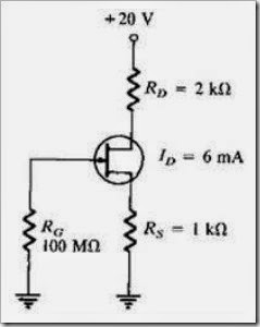
18. Refer to Figure 8-3. Determine the value of VS.

MCQs in  Field-Effect Transistors (FETs) Fig. 03

Figure 8-3

  • A) 20 V
  • B) 8 V
  • C) 6 V
  • D) 2 V

19. Refer to Figure 8-3. Calculate the value of VD.

  • A) 20 V
  • B) 8 V
  • C) 6 V
  • D) 2 V

20. Refer to Figure 8-3. What is the value of IG?

  • A) 6 mA
  • B) 4 mA
  • C) 2 mA
  • D) 0 mA

21. Refer to Figure 8-3. Determine the value of VGS.

  • A) –20 V
  • B) –8 V
  • C) –6 V
  • D) –2 V

22. Refer to Figure 8-3. Calculate the value of VDS.

  • A) 0 V
  • B) 2 V
  • C) 4 V
  • D) –2 V

23. The JFET is always operated with the gate-source pn junction _____ -biased.

  • A) forward
  • B) reverse

24. What three areas are the drain characteristics of a JFET (VGS = 0) divided into?

  • A) ohmic, constant-current, breakdown
  • B) pinch-off, constant-current, avalanche
  • C) ohmic, constant-voltage, breakdown

25. What type(s) of gate-to-source voltage(s) can a depletion MOSFET (D-MOSFET) operate with?

  • A) zero
  • B) positive
  • C) negative
  • D) any of the above

26. The _____ has a physical channel between the drain and source.

  • A) D-MOSFET
  • B) E-MOSFET
  • C) V-MOSFET

27. All MOSFETs are subject to damage from electrostatic discharge (ESD).

  • A) true
  • B) false

28. Midpoint bias for a D-MOSFET is ID = _____, obtained by setting VGS = 0.

  • A) IDSS / 2
  • B) IDSS / 3.4
  • C) IDSS

29. In a self-biased JFET circuit, if VD = VDD then ID = _____.

  • A) 0
  • B) cannot be determined from information above

30. If VD is less than expected (normal) for a self-biased JFET circuit, then it could be caused by a(n)

  • A) open RG.
  • B) open gate lead.
  • C) FET internally open at gate.
  • D) all of the above

31. The resistance of a JFET biased in the ohmic region is controlled by

  • A) VD.
  • B) VGS.
  • C) VS.
  • D) VDS.

Back to Homepage


credit: Thomas L. Floyd©2013 www.FroydWess.com

Power Amplifiers - MCQs Answers

1 comments Posted by Unknown at 11:09 AM
Hits:
Answers key for Power Amplifiers
Below are the answers key for the Multiple Choice Questions (Quiz) in Power Amplifiers.

1. because the collector terminal is the critical terminal for heat dissipation

2. with no signal input

3. slightly less than 180° of the input cycle

4. thermal runaway

5. class C

6. class B

7. 750

8. class C

9. 4.4 mA

10. 5.4 V

11. class A

12. class AB

13. 0.7 V, 15 V, 0 V

14. about 78%

15. 10.7 V

16. 9.3 V

17. C3 is open

18. BE1 is open

19. R1 is open

20. VCC is 0 V

21. a sine wave.

22. 10

23. B

24. AB

25. 79

26. AB

27. C

28. all of the above

29. both of the above

30. B

Back to Homepage


credit: Thomas L. Floyd©2013 www.FroydWess.com

Power Amplifiers - MCQs

0 comments Posted by Unknown at 11:01 AM
Hits:
MCQs for Power Amplifiers

Multiple Choice Questions Topic Outline

  • MCQs in Power Amplifiers
  • MCQs in Class A Power Amplifier
  • MCQs in Class A Power Amplifier
  • MCQs in Class AB Push-Pull Amplifiers
  • MCQs in Class C Power Amplifier

Begin and Good luck!

1. For BJT power transistors, the collector terminal is always connected to the transistor's case

  • A) for easy circuit connection.
  • B) to prevent shorts.
  • C) because the collector terminal is the critical terminal for heat dissipation.
  • D) because the collector terminal is located nearest the case.

2. Quiescent power is the power dissipation of a transistor

  • A) with no signal input.
  • B) with no load.
  • C) under full load.
  • D) along the dc load line.

3. A class B amplifier operates in the linear region for

  • A) slightly more than 180° of the input cycle.
  • B) 360° of the input cycle.
  • C) slightly less than 180° of the input cycle.
  • D) much less than 180° of the input cycle.

4. In a class AB amplifier, if the VBE drops are not matched to the diode drops or if the diodes are not in thermal equilibrium with the transistors, this can result in

  • A) a current mirror.
  • B) diode separation.
  • C) crossover distortion.
  • D) thermal runaway.

5. Which amplifier is commonly used as a frequency multiplier?

  • A) class A
  • B) class B
  • C) class C
  • D) all of the above

6. The least efficient amplifier among all classes is

  • A) class B.
  • B) class A.
  • C) class AB.
  • D) class C.

7. A class A amplifier has a voltage gain of 30 and a current gain of 25. What is the power gain?

  • A) 30
  • B) 25
  • C) 1.2
  • D) 750

8. You have an application for a power amplifier to operate on FM radio frequencies. The most likely choice would be a _____ amplifier.

  • A) class A
  • B) class B
  • C) class C
  • D) class AB

9. A class A amplifier with RC = 3.3 kΩ and RE = 1.2 kΩ has a VCC = 20 V. Find IC(sat).

  • A) 4.4 mA
  • B) 6.1 mA
  • C) 16.7 mA
  • D) 20 mA

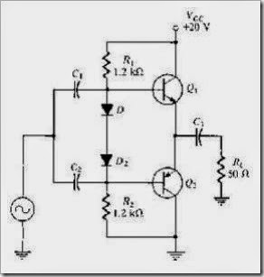
10. Refer to Figure 7-1. The dc voltage on the collector, VC, is

MCQs in Power Amplifiers Fig. 01

Figure 7-1

  • A) 5.4 V.
  • B) 6.6 V.
  • C) 12 V.
  • D) 0 V.

11. Refer to Figure 9-1. This amplifier is operating as a _____ amplifier.

  • A) class A
  • B) class B
  • C) class AB
  • D) class C

12. Refer to Figure 7-2. This amplifier is operating as a _____ amplifier.

MCQs in Power Amplifiers Fig. 02

Figure 7-2

  • A) class A
  • B) class B
  • C) class AB
  • D) class C

13. Refer to Figure 7-2. The approximate voltages on the base, collector, and emitter, respectively, are

  • A) 0.7 V, 6.8 V, 0 V.
  • B) 0 V, 0 V, 0 V.
  • C) 0.7 V, 15 V, 0 V.
  • D) 0.7 V, 0 V, 15 V.

14. Refer to Figure 7-2. The maximum efficiency of this amplifier is

  • A) about 25%.
  • B) about 78%.
  • C) about 70%.
  • D) about 100%.

15. Refer to Figure 7-3. Determine VB1.

MCQs in Power Amplifiers Fig. 03

Figure 7-3

  • A) 0 V
  • B) 0.7 V
  • C) 9.3 V
  • D) 10.7 V

16. Refer to Figure 7-3. Calculate VB2.

  • A) 0 V
  • B) 0.7 V
  • C) 9.3 V
  • D) 10.7 V

17. Refer to Figure 7-3. You have an oscilloscope across RL and it shows a zero signal voltage. The problem might be that

  • A) C3 is open.
  • B) BE1 is open.
  • C) BE2 is open.
  • D) R1 is open.

18. Refer to Figure 7-3. You find that this amplifier only shows the negative alternation at the output. The possible trouble might be that

  • A) C3 is shorted.
  • B) BE1 is open.
  • C) BE2 is open.
  • D) R1 is open.

19. Refer to Figure 7-3. You find that there is no output signal. You measure the dc voltage of Q1 emitter and find it equal to 0 V. The trouble might be

  • A) D1 is shorted.
  • B) D2 is shorted.
  • C) R1 is open.
  • D) no trouble, everything is normal.

20. Refer to Figure 7-3. You find that there is an input signal on the base of Q1 and Q2. However, there is no output signal. You then measure the dc voltages on Q2 and find them to be all 0 V. The possible trouble might be

  • A) C3 is shorted.
  • B) C1 is open.
  • C) RL is shorted.
  • D) VCC is 0 V.

21. A class C amplifier has a tank circuit in the output. The amplifier is conducting only 28°. The output voltage is

  • A) 0 V.
  • B) a dc value equal to VCC.
  • C) a sine wave.
  • D) a square wave with a frequency determined by the tank.

22. In practice, the efficiency of a capacitively coupled class A amplifier is about _____%.

  • A) 25
  • B) 40
  • C) 70
  • D) 10

23. The Q-point is at cutoff for class _____ operation.

  • A) A
  • B) B
  • C) C
  • D) AB

24. Class _____ amplifiers are normally operated in a push-pull configuration in order to produce an output that is a replica of the input.

  • A) A
  • B) B
  • C) C
  • D) AB

25. The maximum efficiency of a class B amplifier is _____ percent.

  • A) 50
  • B) 25
  • C) 70
  • D) 79

26. A class _____ amplifier is biased slightly above cutoff and operates in the linear region for slightly more than 180º of the input cycle.

  • A) A
  • B) B
  • C) C
  • D) AB

27. Which class of amplifier operates in the linear region for only a small part of the input cycle?

  • A) A
  • B) B
  • C) C
  • D) AB

28. The principal advantage(s) of MOSFETs over BJTs is (are)

  • A) their biasing networks are simpler.
  • B) their drive requirements are simpler.
  • C) they can be connected in parallel for added drive capability.
  • D) all of the above

29. The principal advantage(s) of BJTs over MOSFETs is (are) that

  • A) voltage drop across the transistor is important.
  • B) they are not as prone to ESD.
  • C) both of the above
  • D) none of the above

30. The class _____ amplifier is biased below cutoff.

  • A) A
  • B) AB
  • C) B
  • D) C

Back to Homepage

Note: Check your works. Power Amplifiers - MCQs Answers

credit: Thomas L. Floyd©2013 www.FroydWess.com

Sunday, April 13, 2014

Bipolar Junction Transistor Amplifiers - MCQs Answers

0 comments Posted by Unknown at 5:44 PM
Hits:
Answers key for  Floyd's Bipolar Junction Transistor Amplifiers
Below are the answers key for the Multiple Choice Questions (Quiz) in Bipolar Junction Transistor Amplifiers .

1. effectively shorts

2. to maximize amplifier gain

3. to reduce the effects of r'e

4. common-collector amplifier

5. emitter

6. the difference of the two input voltages

7. two inputs and two outputs

8. 3.125 Ω

9. 3.7 V

10. 6 mA

11. 5 V

12. 50 kΩ

13. 3.77 kΩ

14. 5

15. 416 Ω

16. 378 Ω

17. 600

18. 12 mV

19. an open C2.

20. an open base-emitter of Q1

21. a low voltage gain and a high input impedance

22. common-emitter

23. re

24. high, high, high, low

25. replace coupling and bypass capacitors with opens

26. decreases

27. high, high, low

28. multiplication, increased

29. sum of dB voltage gains

30. hre / hoe

31. less input voltage is needed to turn it on.

Back to Homepage


credit: Thomas L. Floyd©2013 www.FroydWess.com

Bipolar Junction Transistor Amplifiers - MCQs

0 comments Posted by Unknown at 5:38 PM
Hits:
MCQs for Floyd's Bipolar Junction Transistor Amplifiers

Multiple Choice Questions Topic Outline

  • MCQs in BJT Amplifiers
  • MCQs in Amplifier Operation
  • MCQs in Transistor AC Models
  • MCQs in The Common-Emitter Amplifier
  • MCQs in The The Common-Collector Amplifier
  • MCQs in The The Common-Base Amplifier
  • MCQs in Multistage Amplifiers
  • MCQs in The Differential Amplifier
  • MCQs in GreenTech Application 6: Wind Power

Begin and Good luck!

1. For the common-emitter amplifier ac equivalent circuit, all capacitors are

  • A) effectively shorts.
  • B) effectively open circuits.
  • C) not connected to ground.
  • D) connected to ground.

2. For a common-emitter amplifier, the purpose of the emitter bypass capacitor is

  • A) no purpose, since it is shorted out by RE.
  • B) to reduce noise.
  • C) to despike the supply voltage.
  • D) to maximize amplifier gain.

3. For a common-emitter amplifier, the purpose of swamping is

  • A) to minimize gain.
  • B) to reduce the effects of r'e
  • C) to maximize gain.
  • D) no purpose.

4. An emitter-follower is also known as a

  • A) common-emitter amplifier.
  • B) common-base amplifier.
  • C) common-collector amplifier.
  • D) Darlington pair.

5. In a common-base amplifier, the input signal is connected to the

  • A) base.
  • B) collector.
  • C) emitter.
  • D) output.

6. The differential amplifier produces outputs that are

  • A) common mode.
  • B) in-phase with the input voltages.
  • C) the sum of the two input voltages.
  • D) the difference of the two input voltages.

7. The differential amplifier has

  • A) one input and one output.
  • B) two inputs and two outputs.
  • C) two inputs and one output.
  • D) one input and two outputs.

8. The dc emitter current of a transistor is 8 mA. What is the value of re?

  • A) 320 Ω
  • B) 13.3 kΩ
  • C) 3.125 Ω
  • D) 5.75 Ω

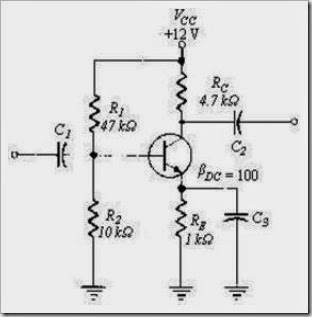
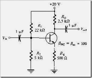
9. Refer to Figure 6-1. Calculate the value of VB.

MCQs in Floyd's Bipolar Junction Transistor Amplifiers Fig. 01

Figure 6-1

  • A) 5 V
  • B) 3.7 V
  • C) 20 V
  • D) 3 V

10. Refer to Figure 6-1. Find the value of IE.

  • A) 2 mA
  • B) 4 mA
  • C) 5 mA
  • D) 6 mA

11. Refer to Figure 6-1. Determine the value of VC.

  • A) 20 V
  • B) 10 V
  • C) 5 V
  • D) 0 V

12. Refer to Figure 6-1. Find the value of Rin(base).

  • A) 420 Ω
  • B) 50 kΩ
  • C) 940 Ω
  • D) 100.8 Ω

13. Refer to Figure 6-1. Calculate the value of Rin(tot).

  • A) 37.7 kΩ
  • B) 3.77 kΩ
  • C) 378 Ω
  • D) 2.25 kΩ

14. Refer to Figure 6-1. Determine the value of Av.

  • A) 49.6
  • B) 5
  • C) 100
  • D) 595

15. Refer to Figure 6-1. If an emitter bypass capacitor was installed, determine the value of Rin(base).

  • A) 416 Ω
  • B) 5 kΩ
  • C) 50 kΩ
  • D) 500 Ω

16. Refer to Figure 6-1. If an emitter bypass capacitor was installed, calculate the value of Rin(tot).

  • A) 378 Ω
  • B) 420 Ω
  • C) 500 Ω
  • D) 40 k Ω

17. Refer to Figure 6-1. If an emitter bypass capacitor was installed, what would the new Av be?

  • A) 4.96
  • B) 125
  • C) 398
  • D) 600

18. An emitter-follower amplifier has an input impedance of 107 kΩ. The input signal is 12 mV. The approximate output voltage is (common-collector)

  • A) 8.92 V
  • B) 112 mV
  • C) 12 mV
  • D) 8.9 mV

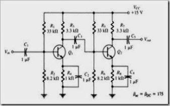
19. Refer to Figure 6-2. You notice while servicing this amplifier that the output signal at Vout is reduced from normal. The problem could be caused by

MCQs in Floyd's Bipolar Junction Transistor Amplifiers Fig. 02

Figure 6-2

  • A) an open C3.
  • B) an open C2.
  • C) an open base-emitter of Q2.
  • D) a shorted C2.

20. Refer to Figure 6-2. The output signal from the first stage of this amplifier is 0 V. The trouble could be caused by

  • A) an open C4.
  • B) an open C2.
  • C) an open base-emitter of Q1.
  • D) a shorted C4.

21. A Darlington pair amplifier has

  • A) high input impedance and high voltage gain.
  • B) low input impedance and low voltage gain.
  • C) a voltage gain of about 1 and a low input impedance.
  • D) a low voltage gain and a high input impedance.

22. You have a need to apply an amplifier with a very high power gain. Which of the following would you choose?

  • A) common-collector
  • B) common-base
  • C) common-emitter
  • D) emitter-follower

23. What is the most important r parameter for amplifier analysis?

  • A) rb
  • B) rc
  • C) re
  • D) none of the above

24. A common-emitter amplifier has _____ voltage gain, _____ current gain, _____ power gain, and _____ input impedance.

  • A) high, low, high, low
  • B) high, high, high, low
  • C) high, high, high, high
  • D) low, low, low, high

25. To analyze the common-emitter amplifier, what must be done to determine the dc equivalent circuit?

  • A) leave circuit unchanged
  • B) replace coupling and bypass capacitors with opens
  • C) replace coupling and bypass capacitors with shorts
  • D) replace VCC with ground

26. When the bypass capacitor is removed from a common-emitter amplifier, the voltage gain

  • A) increases.
  • B) decreases.
  • C) has very little effect.

27. A common-collector amplifier has _____ input resistance, _____ current gain, and _____ voltage gain.

  • A) high, high, low
  • B) high, low, low
  • C) high, low, high

28. A Darlington pair provides beta _____ for _____ input resistance.

  • A) multiplication, decreased
  • B) multiplication, increased
  • C) division, decreased

29. The total gain of a multistage amplifier is the _____.

  • A) sum of individual voltage gains
  • B) sum of dB voltage gains
  • C) none of the above

30. What is re equal to in terms of h parameters?

  • A) hre / hoe
  • B) (hre + 1) / hoe
  • C) hie – (hre / hoe)(1 + hfe)
  • D) hfe
  • E) none of the above

31. The advantage that a Sziklai pair has over a Darlington pair is

  • A) higher current gain.
  • B) less input voltage is needed to turn it on.
  • C) higher input impedance.
  • D) higher voltage gain.

Back to Homepage


credit: Thomas L. Floyd©2013 www.FroydWess.com

Transistor Bias Circuits - MCQs Answers

1 comments Posted by Unknown at 5:09 PM
Hits:
Answers key for   Transistor Bias Circuits
Below are the answers key for the Multiple Choice Questions (Quiz) in Transistor Bias Circuits .

1. collector-feedback bias

2. both positive and negative supply voltages

3. all of the above

4. all of the above

5. only if the base current is much larger than the current through R2 (the lower bias resistor).

6. VC = 8.75 V

7. halfway between cutoff and saturation.

8. 50 µA

9. 5 mA

10. 100

11. 5 mA

12. 2.5 V

13. 1.5 kΩ

14. 320 µA

15. RE is open

16. no problems.

17. a short from collector to emitter

18. the base-emitter junction is open

19. voltage-divider bias

20. zero, I(sat)

21. saturation, cutoff

22. voltage-divider

23. βDCRE

24. voltage-divider bias

25. base bias

26. emitter bias

27. collector-feedback bias

28. nonconducting

29. saturated

30. cutoff

Back to Homepage


credit: Thomas L. Floyd©2013 www.FroydWess.com

Transistor Bias Circuits - MCQs

0 comments Posted by Unknown at 5:04 PM
Hits:
MCQs for  Transistor Bias Circuits

Multiple Choice Questions Topic Outline

  • MCQs in Transistor Bias Circuits
  • MCQs in The DC Operating Point
  • MCQs in Voltage-Divider Bias
  • MCQs in Other Bias Methods
  • MCQs in GreenTech Application 5: Wind Power

Begin and Good luck!

1. Voltage-divider bias has a relatively stable Q-point, as does

  • A) base bias.
  • B) collector-feedback bias.
  • C) both of the above
  • D) none of the above

2. Emitter bias requires

  • A) only a positive supply voltage.
  • B) only a negative supply voltage.
  • C) no supply voltage.
  • D) both positive and negative supply voltages.

3. Clipping is the result of

  • A) the input signal being too large.
  • B) the transistor being driven into saturation.
  • C) the transistor being driven into cutoff.
  • D) all of the above

4. Changes in βDC result in changes in

  • A) IC.
  • B) VCE.
  • C) the Q-point.
  • D) all of the above

5. The input resistance at the base of a voltage-divider biased transistor can be neglected

  • A) at all times.
  • B) only if the base current is much smaller than the current through R2 (the lower bias resistor).
  • C) at no time.
  • D) only if the base current is much larger than the current through R2 (the lower bias resistor).

6. What is the Q-point for a fixed-bias transistor with IB = 75 µA, βDC = 100, VCC = 20 V, and RC = 1.5 kΩ?

  • A) VC = 0 V
  • B) VC = 20 V
  • C) VC = 8.75 V
  • D) VC = 11.25 V

7. Ideally, for linear operation, a transistor should be biased so that the Q-point is

  • A) near saturation.
  • B) near cutoff.
  • C) where IC is maximum.
  • D) halfway between cutoff and saturation.

8. Refer to Figure 5-1. The value of IB is

MCQs in  Transistor Bias Circuits  Fig. 01

Figure 5-1

  • A) 53 µA.
  • B) 50 µA.
  • C) 50 mA.
  • D) 53 mA.

9. Refer to Figure 5-1. The value of IC is

  • A) 10 µA.
  • B) 10 mA.
  • C) 5 mA.
  • D) 50 mA.

10. Refer to Figure 5-1. The value of βDC is

  • A) 5.3.
  • B) 53.
  • C) 94.
  • D) 100.

11. Refer to Figure 5-2. Determine IC.
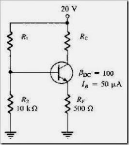
MCQs in  Transistor Bias Circuits  Fig. 02

Figure 5-2

  • A) 5 µA
  • B) 5 mA
  • C) 0 mA
  • D) 10 mA

12. Refer to Figure 5-2. Assume that IC ≈ IE. Find VE.

  • A) 5 V
  • B) 10 V
  • C) 15 V
  • D) 2.5 V

13. Refer to Figure 5-2. Assume IC ≈ IE. Determine the value of RC that will allow VCE to equal 10 V.

  • A) 1 kΩ
  • B) 1.5 kΩ
  • C) 2 kΩ
  • D) 2.5 kΩ

14. Refer to Figure 5-2. Calculate the current I2.

  • A) 32 mA
  • B) 3.2 mA
  • C) 168 µA
  • D) 320 µA

15. Refer to Figure 5-3(a). The most probable cause of trouble, if any, from these voltage measurements would be

MCQs in  Transistor Bias Circuits  Fig. 03
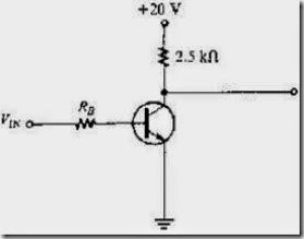
Figure 5-3

  • A) the base-emitter junction is open.
  • B) RE is open.
  • C) a short from collector to emitter.
  • D) no problems.

16. Refer to Figure 5-3(b). The most probable cause of trouble, if any, from these voltage measurements is

  • A) the base-emitter junction is open.
  • B) RE is open.
  • C) a short from collector to emitter.
  • D) no problems.

17. Refer to Figure 5-3(c). The most probable cause of trouble, if any, from these voltage measurements is

  • A) the base-emitter junction is open.
  • B) RE is open.
  • C) a short from collector to emitter.
  • D) no problems.

18. Refer to Figure 5-3(d). The most probable cause of trouble, if any, from these voltage measurements is

  • A) the base-emitter junction is open.
  • B) RE is open.
  • C) a short from collector to emitter.
  • D) no problems.

19. The most stable biasing technique used is the

  • A) voltage-divider bias.
  • B) base bias.
  • C) emitter bias.
  • D) collector bias.

20. At saturation the value of VCE is nearly _____, and IC = _____.

  • A) zero, zero
  • B) VCC, IC(sat)
  • C) zero, I(sat)
  • D) VCC, zero

21. The linear (active) operating region of a transistor lies along the load line below _____ and above _____.

  • A) cutoff, saturation
  • B) saturation, cutoff

22. What is the most common bias circuit?

  • A) base
  • B) collector
  • C) emitter
  • D) voltage-divider

23. What is the dc input resistance at the base of a BJT?

  • A) βDCRC
  • B) βdc • (RC || RE)
  • C) βDC • re
  • D) βDCRE

24. Which transistor bias circuit provides good Q-point stability with a single-polarity supply voltage?

  • A) base bias
  • B) collector-feedback bias
  • C) voltage-divider bias
  • D) emitter bias

25. Which transistor bias circuit arrangement has poor stability because its Q-point varies widely with βDC?

  • A) base bias
  • B) collector-feedback bias
  • C) voltage-divider bias
  • D) emitter bias

26. Which transistor bias circuit arrangement provides good Q-point stability, but requires both positive and negative supply voltages?

  • A) base bias
  • B) collector-feedback bias
  • C) voltage-divider bias
  • D) emitter bias

27. Which transistor bias circuit arrangement provides good stability using negative feedback from collector to base?

  • A) base bias
  • B) collector-feedback bias
  • C) voltage-divider bias
  • D) emitter bias

28.

MCQs in  Transistor Bias Circuits  Fig. 04

FIGURE 5-4

Refer to Figure 5-4. In the voltage-divider biased npn transistor circuit, if RC opens, the transistor is

  • A) saturated.
  • B) cutoff.
  • C) nonconducting.

29. Refer to Figure 5-4. In the voltage-divider biased npn transistor circuit, if R2 opens, the transistor is

  • A) saturated.
  • B) cutoff.
  • C) nonconducting.

30. Refer to Figure 5-4. In the voltage-divider biased npn transistor circuit, if R1 opens, the transistor is

  • A) saturated.
  • B) cutoff.
  • C) nonconducting.

Back to Homepage


credit: Thomas L. Floyd©2013 www.FroydWess.com

Saturday, April 12, 2014

Bipolar Junction Transistors - MCQs Answers

0 comments Posted by Unknown at 12:02 PM
Hits:
Answers key for  Bipolar Junction Transistors
Below are the answers key for the Multiple Choice Questions (Quiz) in Bipolar Junction Transistors .

1. all of the above

2. hfe

3. saturation and cutoff

4. 0.7 V

5. varies with temperature and IC.

6. bipolar junction transistor

7. 3.75 mA

8. 90

9. negative, positive

10. 7.5 V

11. 4.375 V

12. 0.7 V

13. 9.9 V

14. –9.2 V

15. 2.085 mA

16. 10.425 A

17. 13.21 V

18. 7.92 mA

19. 92 kΩ

20. cutoff

21. operating in saturation.

22. emitter, collector, base

23. npn and pnp

24. IE = IB + IC

25. either βDC or hFE, but not αDC

26. either βDC / (βDC + 1) or αDC, but not βDC

27. 0.7 < VCE < VCE(max)

28. both IC and ºC

29. all of the above

30. all of the above

31. nA

Back to Homepage


credit: Thomas L. Floyd©2013 www.FroydWess.com

Bipolar Junction Transistors - MCQs
0 comments Posted by Unknown at 11:56 AM
Hits:
MCQs for Bipolar Junction Transistors

Multiple Choice Questions Topic Outline

  • MCQs in Bipolar Junction Transistor (BJT) Structure
  • MCQs in Basic BJT Operation
  • MCQs in BJT Characteristics and Parameters
  • MCQs in The BJT as an Amplifier
  • MCQs in The Phototransistor
  • MCQs in The BJT as a Switch
  • MCQs in Transistor Categories and Packaging
  • MCQs in GreenTech Application 4: Solar Power

Begin and Good luck!

1. The dc load line on a family of collector characteristic curves of a transistor shows the

  • A) saturation region.
  • B) cutoff region.
  • C) active region.
  • D) all of the above

2. A transistor data sheet usually identifies βDC as

  • A) hre.
  • B) hfe.
  • C) IC.
  • D) VCE.

3. When a transistor is used as a switch, it is stable in which two distinct regions?

  • A) saturation and active
  • B) active and cutoff
  • C) saturation and cutoff
  • D) none of the above

4. For a silicon transistor, when a base-emitter junction is forward-biased, it has a nominal voltage drop of

  • A) 0.7 V.
  • B) 0.3 V.
  • C) 0.2 V.
  • D) VCC.

5. The value of βDC

  • A) is fixed for any particular transistor.
  • B) varies with temperature.
  • C) varies with IC.
  • D) varies with temperature and IC.

6. The term BJT is short for

  • A) base junction transistor.
  • B) binary junction transistor.
  • C) both junction transistor.
  • D) bipolar junction transistor.

7. A BJT has an IB of 50 µA and a βDC of 75; IC is:

  • A) 375 mA
  • B) 37.5 mA
  • C) 3.75 mA
  • D) 0.375 mA

8. A certain transistor has IC = 15 mA and IB = 167 µA; βDC is:

  • A) 15
  • B) 167
  • C) 0.011
  • D) 90

9. For normal operation of a pnp BJT, the base must be _____ with respect to the emitter and _____ with respect to the collector.

  • A) positive, negative
  • B) positive, positive
  • C) negative, positive
  • D) negative, negative

10. A transistor amplifier has a voltage gain of 100. If the input voltage is 75 mV, the output voltage is:

  • A) 1.33 V
  • B) 7.5 V
  • C) 13.3 V
  • D) 15 V

11. A 35 mV signal is applied to the base of a properly biased transistor with an r'e = 8 Ω and RC = 1 kΩ. The output signal voltage at the collector is:

  • A) 3.5 V
  • B) 28.57 V
  • C) 4.375 V
  • D) 4.375 mV

12. Refer to Figure 4-1; the value of VBE is:

MCQs in Bipolar Junction Transistors Fig. 01

Figure 4-1

  • A) 0.6 V
  • B) 0.7 V
  • C) 1.2 V
  • D) 0.079 V

13. Refer to Figure 4-1; the value of VCE is:

  • A) 9.9 V
  • B) 9.2 V
  • C) 0.7 V
  • D) 19.3 V

14. Refer to Figure 4-1; the value of VBC is:

  • A) 9.2 V
  • B) 9.9 V
  • C) –9.9 V
  • D) –9.2 V

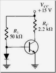
15. Refer to Figure 4-2; if VCE = 0.2 V, IC(sat) is:

MCQs in Bipolar Junction Transistors Fig. 02

Figure 4-2

  • A) 0.05 mA
  • B) 2.085 mA
  • C) 1.065 mA
  • D) 7.4 mA

16. Refer to Figure 4-2. Determine the minimum value of IB that will produce saturation.

  • A) 0.25 mA
  • B) 5.325 A
  • C) 1.065 A
  • D) 10.425 A

17. Refer to Figure 4-2. Determine the minimum value of VIN from the following that will saturate this transistor.

  • A) 13.21 V
  • B) 12.51 V
  • C) 0.7 V
  • D) 9.4 V

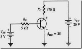
18. Refer to Figure 4-3. The value of βDC = 100 and VIN = 8 V. Determine IC(sat).

MCQs in Bipolar Junction Transistors Fig. 03

Figure 4-3

  • A) 18 mA
  • B) 7.92 mA
  • C) 1.8 mA
  • D) 8 A

19. Refer to Figure 4-3. In this circuit βDC = 100 and VIN = 8 V. The value of RB that will produce saturation is:

  • A) 92 kΩ
  • B) 9.1 MΩ
  • C) 100 kΩ
  • D) 150 kΩ

20. Refer to Figure 4-3. The measured voltage, VCE, is 20 V. The transistor is in

  • A) saturation.
  • B) cutoff.
  • C) normal.
  • D) not enough data.

21. Refer to Figure 4-3. You measure VCE and find it nearly equal to zero. You now know that the transistor is

  • A) operating in cutoff.
  • B) operating normally.
  • C) operating in saturation.
  • D) operating below cutoff.

22. What is the order of doping, from heavily to lightly doped, for each region?

  • A) base, collector, emitter
  • B) emitter, collector, base
  • C) emitter, base, collector
  • D) collector, emitter, base

23. What are the two types of bipolar junction transistors?

  • A) npn and pnp
  • B) pnn and nnp
  • C) ppn and nnp
  • D) pts and stp

24. Which of the following is true for an npn or pnp transistor?

  • A) IE = IB + IC
  • B) IB = IC+ IE
  • C) IC = IB + IE
  • D) none of the above

25. What is the ratio of IC to IB?

  • A) βDC
  • B) hFE
  • C) αDC
  • D) either βDC or hFE, but not αDC

26. What is the ratio of IC to IE?

  • A) βDC
  • B) βDC / (βDC + 1)
  • C) αDC
  • D) either βDC / (βDC + 1) or αDC, but not βDC

27. In what range of voltages is the transistor in the linear region of its operation?

  • A) 0 < VCE
  • B) 0.7 < VCE < VCE(max)
  • C) VCE(max) > VCE
  • D) none of the above

28. What does DC vary with?

  • A) IC
  • B) ºC
  • C) both IC and ºC
  • D) IC’, but not ºC

29. What is (are) common fault(s) in a BJT-based circuit?

  • A) opens or shorts internal to the transistor
  • B) open bias resistor(s)
  • C) external opens and shorts on the circuit board
  • D) all of the above

30. What is (are) general-purpose/small-signal transistors case type(s)?

  • A) TO-18
  • B) TO-92
  • C) TO-39
  • D) TO-52
  • E) all of the above

31. The magnitude of dark current in a phototransistor usually falls in what range?

  • A) mA
  • B) μA
  • C) nA
  • D) pA

Back to Homepage

Note: Check your works. Bipolar Junction Transistors - MCQs Answers


credit: Thomas L. Floyd©2013 www.FroydWess.com

Special-Purpose Diodes - MCQs Answers

0 comments Posted by Unknown at 11:24 AM
Hits:
Answers key for  Special-Purpose Diodes
Below are the answers key for the Multiple Choice Questions (Quiz) in Special-Purpose Diodes .

1. electroluminescence.

2. reverse-breakdown region.

3. hot carrier diodes.

4. coherent and monochromatic light.

5. 8.325 V.

6. 161 mA.

7. remain the same, decrease

8. increase.

9. increase.

10. decrease.

11. e

12. b

13. d

14. c

15. a

16. the diode is open.

17. in very fast-switching circuits.

18. in circuits requiring negative resistance.

19. a varactor.

20. zener

21. avalanche

22. varactor

23. reverse, maximize

24. gallium.

25. current regulator

26. Schottky

27. Schottky

28. step-recovery

29. LED

30. to eliminate harmonic distortion

Back to Homepage


credit: Thomas L. Floyd©2013 www.FroydWess.com

Special-Purpose Diodes - MCQs

0 comments Posted by Unknown at 11:19 AM
Hits:
MCQs for Special-Purpose Diodes

Multiple Choice Questions Topic Outline

  • MCQs in The Zener Diode
  • MCQs in Zener Diode Applications
  • MCQs in The Varactor Diode
  • MCQs in Optical Diodes
  • MCQs in Other Types of Diodes
  • MCQs in GreenTech Application 3: Solar Power

Begin and Good luck!

1. The process of emitting photons from a semiconductive material is called

  • A) photoluminescence.
  • B) gallium arsenide.
  • C) electroluminescence.
  • D) gallium phosphide.

2. The normal operating region for a zener diode is the

  • A) forward-bias region.
  • B) reverse-bias region.
  • C) zero-crossing region.
  • D) reverse-breakdown region.

3. Schottky diodes are also known as

  • A) PIN diodes.
  • B) hot carrier diodes.
  • C) step-recovery diodes.
  • D) tunnel diodes.

4. A laser diode normally emits

  • A) coherent light.
  • B) monochromatic light.
  • C) coherent and monochromatic light.
  • D) neither coherent nor monochromatic light.

5. An 8.2 V zener has a resistance of 5 Ω. The actual voltage across its terminals when the current is 25 mA is

  • A) 8.2 V.
  • B) 125 mV.
  • C) 8.325 V.
  • D) 8.075 V.

6. A 6.2 V zener is rated at 1 watt. The maximum safe current the zener can carry is

  • A) 1.61 A.
  • B) 161 mA.
  • C) 16.1 mA.
  • D) 1.61 mA.

7. Refer to Figure 3-1. If the load current increases, IR will _____ and IZ will _____.

MCQs in Special-Purpose Diodes Fig. 01

Figure 3-1

  • A) remain the same, increase
  • B) decrease, remain the same
  • C) increase, remain the same
  • D) remain the same, decrease

8. Refer to Figure 3-1. If VIN attempts to increase, VR will

  • A) increase.
  • B) decrease.
  • C) remain the same.

9. Refer to Figure 3-1. If VIN increases, IZ will

  • A) increase.
  • B) decrease.
  • C) remain the same.

10. Refer to Figure 3-1. If VIN decreases, IR will

  • A) increase.
  • B) decrease.
  • C) remain the same.

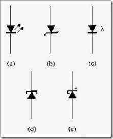
11. Refer to Figure 3-2. Identify the Schottky diode.

MCQs in Special-Purpose Diodes Fig. 02

Figure 3-2

  • A) a
  • B) b
  • C) c
  • D) d
  • E) e

12. Refer to Figure 3-2. Which symbol is correct for a zener diode?

  • A) a
  • B) b
  • C) c
  • D) d
  • E) e

13. Refer to Figure 3-2. Find the tunnel diode symbol.

  • A) a
  • B) b
  • C) c
  • D) d
  • E) e

14. Refer to Figure 3-2. Which symbol is correct for a photodiode?

  • A) a
  • B) b
  • C) c
  • D) d
  • E) e

15. Refer to Figure 3-2. Which symbol is correct for an LED?

  • A) a
  • B) b
  • C) c
  • D) d
  • E) e

16. An LED is forward-biased. The diode should be on, but no light is showing. A possible trouble might be

  • A) the diode is open.
  • B) the series resistor is too small.
  • C) none. The diode should be off if forward-biased.
  • D) the power supply voltage is too high.

17. The Schottky diode is used

  • A) in high-power circuits.
  • B) in circuits requiring negative resistance.
  • C) in very fast-switching circuits.
  • D) in power supply rectifiers.

18. A tunnel diode is used

  • A) in high-power circuits.
  • B) in circuits requiring negative resistance.
  • C) in very fast-switching circuits.
  • D) in power supply rectifiers.

19. You have an application for a diode to be used in a tuning circuit. A type of diode to use might be

  • A) an LED.
  • B) a Schottky diode.
  • C) a Gunn diode.
  • D) a varactor.

20. Zener diodes with breakdown voltages less than 5 V operate predominantly in what type of breakdown?

  • A) avalanche
  • B) zener
  • C) varactor
  • D) Schottky

21. Zener diodes with breakdown voltages greater than 5 V operate predominantly in what type of breakdown?

  • A) avalanche
  • B) zener
  • C) varactor
  • D) Schottky

22. What type of diode is commonly used in electronic tuners in TVs?

  • A) varactor
  • B) Schottky
  • C) LED
  • D) Gunn

23. A varactor is a pn junction diode that always operates in _____-bias and is doped to _____ the inherent capacitance of the depletion region.

  • A) forward, maximize
  • B) reverse, maximize
  • C) reverse, minimize
  • D) forward, minimize

24. LEDs are made out of

  • A) silicon.
  • B) germanium.
  • C) gallium.
  • D) silicon and germanium, but not gallium.

25. What type of diode maintains a constant current?

  • A) LED
  • B) zener
  • C) current regulator
  • D) pin
  • E) none of the above

26. What diode operates only with majority carriers?

  • A) laser
  • B) tunnel
  • C) Schottky
  • D) step-recovery

27. What kind of diode is formed by joining a doped semiconductor region with a metal?

  • A) laser
  • B) tunnel
  • C) pin
  • D) Schottky

28. Which diode employs graded doping?

  • A) zener
  • B) LED
  • C) tunnel
  • D) step-recovery

29. What diode is used in seven-segment displays?

  • A) zener
  • B) LED
  • C) laser
  • D) Schottky

30. Back-to-back varactor diodes are used for what reason?

  • A) over-voltage protection
  • B) a wider tuning range
  • C) to eliminate harmonic distortion
  • D) no reason; only zeners are used in a back-to-back configuration

Back to Homepage

Note: Check your works. Special-Purpose Diodes - MCQs Answers


credit: Thomas L. Floyd©2013 www.FroydWess.com
 

© 2013 - 2014. All Rights Reserved | Online Notes and Lectures | Customized by MovieOnMovie

Home | | | Top