Multiple Choice Questions Topic Outline
- MCQs in FET Devices
- MCQs in Construction and Characteristics of JFETs
- MCQs in Transfer Characteristics
- MCQs in Specification Sheets (JFETs)
- MCQs in Instrumentation
- MCQs in Important Relationships
- MCQs in Depletion-Type MOSFET
- MCQs in Enhancement-Type MOSFET
- MCQs in MOSFET Handling
- MCQs in VMOS
- MCQs in CMOS
Begin and Good luck!
1. Which of the following controls the level of ID?
- A) VGS
- B) VDS
- C) IG
- D) VDG
2. Which of the following is (are) not an FET?
- A) n-channel
- B) p-channel
- C) p-n channel
- D) n-channel and p-channel
3. What is the range of an FET's input impedance?
- A) 10 Ω to 1 kΩ
- B) 1 kΩ to 10 kΩ
- C) 50 kΩ to 100 kΩ
- D) 1 MΩ to several hundred MΩ
4. Which of the following transistor(s) has (have) depletion and enhancement types?
- A) BJT
- B) JFET
- C) MOSFET
- D) None of the above
5. A BJT is a _____-controlled device. The JFET is a _____ - controlled device.
- A) voltage, voltage
- B) voltage, current
- C) current, voltage
- D) current, current
6. The BJT is a _____ device. The FET is a _____ device.
- A) bipolar, bipolar
- B) bipolar, unipolar
- C) unipolar, bipolar
- D) unipolar, unipolar
7. Which of the following is (are) the terminal(s) of a field-effect transistor (FET).
- A) Drain
- B) Gate
- C) Source
- D) All of the above
8. What is the level of IG in an FET?
- A) Zero amperes
- B) Equal to ID
- C) Depends on VDS
- D) Undefined
9. At which of the following is the level of VDS equal to the pinch-off voltage?
- A) When ID becomes equal to IDSS
- B) When VGS is zero volts
- C) IG is zero
- D) All of the above
10. At which of the following condition(s) is the depletion region uniform?
- A) No bias
- B) VDS > 0 V
- C) VDS = VP
- D) None of the above
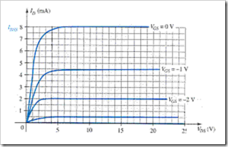
11. Refer to the following characteristic curve. Calculate the resistance of the FET at VGS = –0.25 V if ro = 10 kΩ.
- A) 1.1378 kΩ
- B) 113.78 Ω
- C) 11.378 Ω
- D) 11.378 kΩ
12. What is the level of drain current ID for gate-to-source voltages VGS less than (more negative than) the pinch-off level?
- A) zero amperes
- B) IDSS
- C) Negative value
- D) Undefined
13. The three terminals of the JFET are the _____, _____, and _____.
- A) gate, collector, emitter
- B) base, collector, emitter
- C) gate, drain, source
- D) gate, drain, emitter
14. The level of VGS that results in ID = 0 mA is defined by VGS = _____.
- A) VGS(off)
- B) VP
- C) VDS
- D) None of the above
15. The region to the left of the pinch-off locus is referred to as the _____ region.
- A) saturation
- B) cutoff
- C) ohmic
- D) All of the above
16. Which of the following represent(s) the cutoff region for an FET?
- A) ID = 0 mA
- B) VGS = VP
- C) IG = 0
- D) All of the above
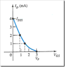
17. Referring to this transfer curve. Calculate (using Shockley's equation) VGS at ID = 4mA.
- A) 2.54 V
- B) –2.54 V
- C) –12 V
- D) Undefined
18. Referring to this transfer curve, determine ID at VGS = 2 V.
- A) 0.444 mA
- B) 1.333 mA
- C) 0.111 mA
- D) 4.444 mA
19. What is the ratio of ID / IDSS for VGS = 0.5 VP?
- A) 0.25
- B) 0.5
- C) 1
- D) 0
20. The drain current will always be one-fourth of IDSS as long as the gate-to-source voltage is _____ the pinch-off value.
- A) one-fourth
- B) one-half
- C) three-fourths
- D) None of the above
21. Which of the following ratings appear(s) in the specification sheet for an FET?
- A) Voltages between specific terminals
- B) Current levels
- C) Power dissipation
- D) All of the above
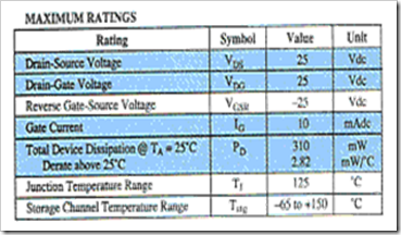
22. Refer to this portion of a specification sheet. Determine the values of reverse-gate-source voltage and gate current if the FET was forced to accept it.
- A) 25 Vdc, –200 nAdc
- B) –25 Vdc, 10 mAdc
- C) –6 Vdc, –1.0 nAdc
- D) None of the above
23. Hand-held instruments are available to measure _____ for the BJT.
- A) βdc
- B) IDSS
- C) VP
- D) All of the above
24. How many terminals can a MOSFET have?
- A) 2
- B) 3
- C) 4
- D) 3 or 4
25. Which of the following applies to MOSFETs?
- A) No direct electrical connection between the gate terminal and the channel
- B) Desirable high input impedance
- C) Uses metal for the gate, drain, and source connections
- D) All of the above
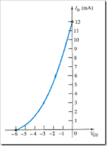
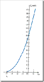
26. Referring to the following transfer curve, determine the level of VGS when the drain current is 20 mA.
- A) 1.66 V
- B) –1.66 V
- C) 0.66 V
- D) –0.66 V
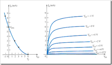
27. Refer to the following curves. Calculate ID at VGS = 1 V.
- A) 8.167 mA
- B) 4.167 mA
- C) 6.167 mA
- D) 0.616 mA
28. It is the insulating layer of _____ in the MOSFET construction that accounts for the very desirable high input impedance of the device.
- A) SiO
- B) GaAs
- C) SiO2
- D) HCl
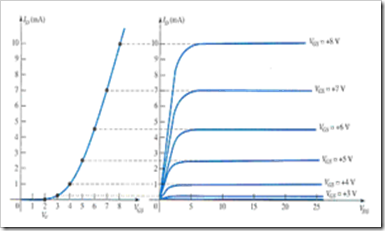
29. Refer to the following figure. Calculate VGS at ID = 8 mA for k = 0.278 × 10⁻² A/V2.
- A) 3.70 V
- B) 5.36 V
- C) 7.36 V
- D) 2.36 V
30. The transfer curve is not defined by Shockley's equation for the _____.
- A) JFET
- B) depletion-type MOSFET
- C) enhancement-type MOSFET
- D) BJT
31. Which of the following applies to a safe MOSFET handling?
- A) Always pick up the transistor by the casing.
- B) Power should always be off when network changes are made.
- C) Always touch ground before handling the device.
- D) All of the above
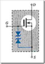
32. What is the purpose of adding two Zener diodes to the MOSFET in this figure?
- A) To reduce the input impedance
- B) To protect the MOSFET for both polarities
- C) To increase the input impedance
- D) None of the above
33. Which of the following is (are) the advantage(s) of VMOS over MOSFETs?
- A) Reduced channel resistance
- B) Higher current and power ratings
- C) Faster switching time
- D) All of the above
34. Which of the following FETs has the lowest input impedance?
- A) JFET
- B) MOSFET depletion-type
- C) MOSFET enhancement-type
- D) None of the above
35. Which of the following input impedances is not valid for a JFET?
- A) 1010 Ω
- B) 109 Ω
- C) 108 Ω
- D) 1011 Ω
Fill-in-the-blanks Questions
1. A junction field-effect transistor (JFET) is a _____ device.
- A) current-controlled
- B) voltage-controlled
- C) voltage-current controlled
- D) None of the above
2. The FET is a _____ device depending solely on either electron (n-channel) or hole (p-channel) conduction.
- A) unipolar
- B) bipolar
- C) tripolar
- D) None of the above
3. One of the most important characteristics of the FET is its _____ impedance.
- A) low input
- B) medium input
- C) high input
- D) None of the above
4. The _____ transistor has become one of the most important devices used in the design and construction of integrated circuits for digital computers.
- A) MOSFET
- B) BJT
- C) JFET
- D) None of the above
5. In the n-channel transistor, the drain and source are connected to the _____ channel while the gate is connected to the two layers of _____ material.
- A) p-type, n-type
- B) p-type, p-type
- C) n-type, p-type
- D) n-type, n-type
6. In an FET transistor, the depletion region is _____ near the top of both p-type materials.
- A) wider
- B) narrower
- C) the same as the rest of the depletion region
- D) None of the above
7. The pinch-off voltage continues to drop in a _____ manner as VGS becomes more and more negative.
- A) linear
- B) parabolic
- C) cubic
- D) None of the above
8. The region to the right of the pinch-off locus is commonly referred to as the _____ region.
- A) constant-current
- B) saturation
- C) linear amplification
- D) All of the above
9. As VGS becomes _____ negative, the slope of each curve in the characteristics becomes _____ horizontal corresponding with an increasing resistance level.
- A) less, more
- B) more, less
- C) more, more
- D) None of the above
10. The transfer curve can be obtained by _____.
- A) using Shockley's equation
- B) using both Shockley's equation and by output characteristics
- C) characteristics
- D) None of the above
11. The active region of an FET is bounded by _____.
- A) ohmic region
- B) cutoff region
- C) power line
- D) All of the above
12. A(n) _____ can be used to check the condition of an FET.
- A) digital display meter (DDM)
- B) ohmmeter (VOM)
- C) curve tracer
- D) All of the above
13. In a curve tracer, the _____ reveals the distance between the VGS curves for the n-channel device.
- A) vertical sens.
- B) horizontal sens.
- C) Per step
- D) gm
14. In an FET circuit, _____ is normally the parameter to be determined first.
- A) VGS
- B) VDS
- C) VDG
- D) ID
15. The primary difference between the construction of a MOSFET and an FET is the _____.
- A) construction of the gate connection
- B) low input impedance
- C) threshold voltage
- D) None of the above
16. The primary difference between the construction of depletion-type and enhancement-type MOSFETs is _____.
- A) the size of the transistor
- B) the absence of the channel
- C) the reverse bias junction
- D) All of the above
17. The level of _____ that results in the significant increase in drain current in enhancement-type MOSFETs is called threshold voltage VT’.
- A) VDD
- B) VDS
- C) VGS
- D) VDG
18. In an n-channel enhancement-type MOSFET with a fixed value of VT’, the _____ the level of VGS’, the _____ the saturation level for VDS’.
- A) higher, more
- B) higher, less
- C) lower, lower
- D) None of the above
19. The enhancement-type MOSFET is in the cutoff region if _____.
- A) applied VGS is larger than VGS(Th)
- B) applied VGS is less than or equal to VGS(Th)
- C) VGS has a positive level
- D) None of the above
20. The specification sheet provides _____ to calculate the value of k for enhancement-type MOSFETs.
- A) VGS(on)
- B) ID(on)
- C) VGS(Th)
- D) All of the above
21. _____ has high input impedance, fast switching speeds, and lower operating power levels.
- A) CMOS
- B) FET
- C) BJT
- D) None of the above
22. The FET resistance in the ohmic region is _____ at VP and _____ at the origin.
- A) smallest, largest
- B) largest, smallest
- C) larger, smaller
- D) smaller, larger
23. The silicon dioxide (SiO2) layer used in a MOSFET is _____.
- A) an insulator
- B) a conductor
- C) a semiconductor
- D) None of the above
24. In an n-channel depletion-type MOSFET the region of positive gate voltages on the drain or transfer characteristics is referred to as the _____ region with the region between cutoff and the saturation level of ID referred to as the _____ region.
- A) depletion, enhancement
- B) enhancement, enhancement
- C) enhancement, depletion
- D) None of the above
25. VMOS FETs have a _____ temperature coefficient that will combat the possibility of thermal runaway.
- A) positive
- B) negative
- C) zero
- D) None of the above
Back to Homepage
Note: Check your works. Field Effect Transistor Devices - MCQs Answers




0 comments: Post Yours! Read Comment Policy ▼
PLEASE NOTE:
I have Zero Tolerance to Spam. It will be deleted immediately upon review.
Post a Comment