Multiple Choice Questions Topic Outline
- MCQs in DC Biasing - Field Effect Transistor
- MCQs in Fixed-Bias Configuration
- MCQs in Self-Bias Configuration
- MCQs in Voltage-Divider Biasing
- MCQs in Depletion-Type MOSFETs
- MCQs in Enhancement-Type MOSFETs
- MCQs in Summary Table
- MCQs in Combination Networks
- MCQs in Design
- MCQs in P-Channel FETs
- MCQs in Universal JFET Bias Curve
Begin and Good luck!
1. What is the approximate current level in the gate of an FET in dc analysis?
- A) 0 A
- B) 0.7 mA
- C) 0.3 mA
- D) Undefined
2. Which of the following current equations is true?
- A) IG = ID
- B) IG = IS
- C) ID = IS
- D) IG = ID = IS
3. For the FET, the relationship between the input and output quantities is _____ due to the _____ term in Shockley's equation.
- A) nonlinear, cubed
- B) linear, proportional
- C) nonlinear, squared
4. The input controlling variable for a(n) _____ is a current level and a voltage level for a(n) _____.
- A) BJT, FET
- B) FET, BJT
- C) FET, FET
- D) BJT, BJT
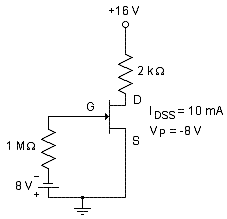
5. Calculate the value of VDS.
- A) 0 V
- B) 8 V
- C) 4.75 V
- D) 16 V
6. The self-bias configuration eliminates the need for two dc supplies.
- A) True
- B) False
7. Which of the following is (are) true of a self-bias configuration compared to a fixed-bias configuration?
- A) One of the dc supplies is eliminated.
- B) A resistor RS is added.
- C) VGS is a function of the output current ID.
- D) All of the above
8. Which of the following represents the voltage level of VGS in a self-bias configuration?
- A) VG
- B) VGS(off)
- C) VS
- D) VP
9. What is the new value of RD when there is 7 V across VDS?
- A) 3 kΩ
- B) 3.3 kΩ
- C) 4 kΩ
- D) 5 kΩ
10. Which of the following is a false statement regarding the dc load line when comparing self-bias and voltage-divider configurations?
- A) Both are linear lines.
- B) Both cross the origin.
- C) Both intersect the transfer characteristics.
- D) Both are obtained by writing Kirchhoff's voltage law (KVL) at the input side loop.
11. For what value of RD is the voltage across VDS zero?
- A) 2.400 kΩ
- B) 5.167 kΩ
- C) 6.167 kΩ
- D) 6.670 kΩ
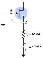
12. Calculate the value of VDS’.
- A) 0 V
- B) 0.35 V
- C) 3.8 V
- D) 33.5 V
13. Which of the following describe(s) the difference(s) between JFETs and depletion-type MOSFETs?
- A) VGS can be positive or negative for the depletion-type.
- B) ID can exceed IDSS for the depletion-type.
- C) The depletion-type can operate in the enhancement mode.
- D) All of the above
14. At what value of RS does the circuit switch from depletion mode to enhancement mode?
- A) 250 Ω
- B) 500 Ω
- C) 10 MΩ
- D) None of the above
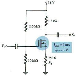
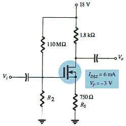
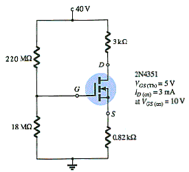
15. For what value of R2 is VGSQ equal to 1 V?
- A) 10 MΩ`
- B) 100 MΩ
- C) 110 MΩ
- D) 220 MΩ
16. Depletion-type MOSFETs do not permit operating points with positive values of VGS and levels of ID that exceed IDSS.
- A) True
- B) False
17. For what value of RS can the depletion-type MOSFETs operate in enhancement mode?
- A) 2.4 kΩ
- B) 5 kΩ
- C) 6.2 kΩ
- D) None of the above
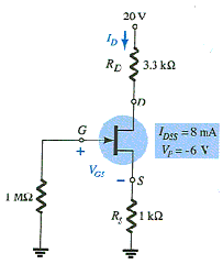
18. Determine the value of VDSQ.
- A) 3.5 V
- B) 4.86 V
- C) 7.14 V
- D) 10 V
19. Calculate the value of VDSQ.
- A) 0 V
- B) 20 V
- C) 30 V
- D) 40 V
20. What are the voltages across RD and RS?
- A) 0 V, 0 V
- B) 5 V, 5 V
- C) 10 V, 10 V
- D) 20 V, 20 V
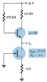
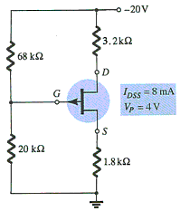
21. Calculate VD.
- A) 23.0 V
- B) 17.0 V
- C) 4.6 V
- D) 12.4 V
22. Specification sheets typically provide the value of the constant k for enhancement-type MOSFETs.
- A) True
- B) False
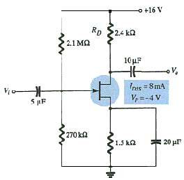
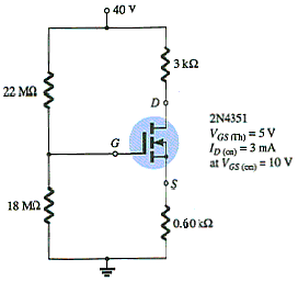
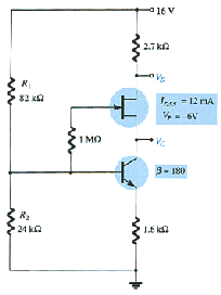
23. Calculate VDS'.
- A) 0 V
- B) 6 V
- C) 16 V
- D) 11 V
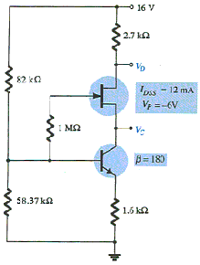
24. Calculate VCE’.
- A) 0 V
- B) 2 V
- C) 3 V
- D) 5.34 V
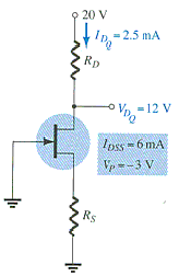
25. Given the values of VDQ and IDQ for this circuit, determine the required values of RD and RS.
- A) 2 kΩ, 2 kΩ
- B) 1 kΩ, 5.3 kΩ
- C) 3.2 kΩ, 400 Ω
- D) 2.5 kΩ, 5.3 kΩ
26. Calculate the value of RS. Assume VGSQ = −2V.
- A) 0 kΩ
- B) 1.68 kΩ
- C) 6.81 kΩ`
- D) 8.5 kΩ
27. Calculate the value of RD’.
- A) 2 kΩ
- B) 3 kΩ
- C) 3.5 kΩ
- D) 4.13 kΩ
28. In the design of linear amplifiers, it is good design practice to choose operating points that do not crowd the saturation level or cutoff regions.
- A) True
- B) False
29. Seldom are current levels measured since such maneuvers require disturbing the network structure to insert the meter.
- A) True
- B) False
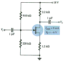
30. Calculate the value of VDS.
- A) –3 V
- B) 3 V
- C) –4 V
- D) 4 V
31. Determine the quiescent values of ID and VGS.
- A) 1.2 mA, –1.8 V
- B) 1.5 mA, –1.5 V
- C) 2.0 mA, –1.2 V
- D) 3.0 mA, –0.8 V
32. Calculate VDSQ.
- A) 1.0 V
- B) 1.50 V
- C) 2.56 V
- D) 3.58 V
33. On the universal JFET bias curve, the vertical scale labelled _____ can, in itself, be used to find the solution to _____ configurations.
- A) m, fixed-bias
- B) M, fixed-bias
- C) M, voltage-bias
- D) m, voltage-bias
34. Through proper design, a ______ can be introduced that will affect the biasing level of a voltage-controlled JFET resistor.
- A) photodiode
- B) thermistor
- C) laser diode
- D) Zener diode
35. For the noninverting amplifier, one of the most important advantages associated with using a JFET for control is the fact that it is _____ rather than _____ control.
- A) dc, ac
- B) ac, dc
Fill-in-the-blanks Questions
1. For the field-effect transistor, the relationship between the input and the output quantities is _____.
- A) linear
- B) nonlinear
- C) 3rd degree
- D) None of the above
2. The input controlling variable for an FET transistor is a _____ level.
- A) resistor
- B) current
- C) voltage
- D) All of the above
3. The controlled variable on the output side of an FET transistor is a _____ level.
- A) current
- B) voltage
- C) resistor
- D) None of the above
4. For _____, Shockley's equation is applied to relate the input and the output quantities.
- A) JFETs
- B) depletion-type MOSFETs
- C) enhancement-type MOSFETs
- D) JFETs and depletion-type MOSFETs
5. The coupling capacitors are _____ for the dc analysis and _____________ for the ac analysis.
- A) open-circuit, low impedance
- B) short-circuit, low impedance
- C) open-circuit, high impedance
- D) None of the above
6. In a fixed-bias configuration, the voltage level of VGS is equal to _____.
- A) VS
- B) VG
- C) VGS(off)
- D) VP
7. The ratio of current ID to IDSS is equal to _____ for a fixed-bias configuration.
- A) 0
- B) 0.25
- C) 0.5
- D) 1
8. When plotting the transfer characteristics, choosing VGS = 0.5VP will result in a drain current level of _____ IDSS.
- A) 0
- B) 0.25
- C) 0.5
- D) 1
9. The dc load line is drawn using the equation obtained by applying Kirchhoff's voltage law (KVL) at _____ side loop(s) of the circuit.
- A) the output
- B) the input
- C) both the input and output
- D) None of the above
10. The slope of the dc load line in a self-bias configuration is controlled by _____.
- A) VDD
- B) RD
- C) RG
- D) RS
11. _____ levels of RS result in _____ quiescent values of ID and _____ negative values of VGS.
- A) Increased, lower, less
- B) Increased, higher, less
- C) Increased, higher, more
- D) Increased, less, lower
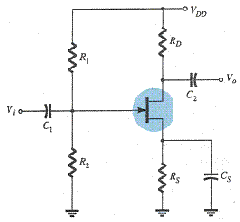
12. The slope of the dc load line in a voltage-divider is controlled by _____.
- A) R1
- B) R2
- C) RS
- D) All of the above
13. In a depletion-type MOSFET, the transfer characteristic rises _____ as VGS becomes more positive.
- A) less rapidly
- B) more rapidly
- C) the same
- D) None of the above
14. In _____ configuration(s) a depletion-type MOSFET can operate in enhancement mode.
- A) self-bias
- B) fixed-bias with no VGG
- C) voltage-divider
- D) None of the above
15. In an enhancement-type MOSFET, the drain current is zero for levels of VGS less than the _____ level.
- A) VGS(Th)
- B) VGS(off)
- C) VP
- D) VDD
16. Specification sheets typically provide _____ for enhancement-type MOSFETs.
- A) the threshold voltage VGS(Th)
- B) a level of drain current ID(on)
- C) an ID(on)
- D) All of the above
17. In a feedback-bias configuration, the slope of the dc load line is controlled by _____.
- A) RG
- B) RD
- C) VDG
- D) None of the above
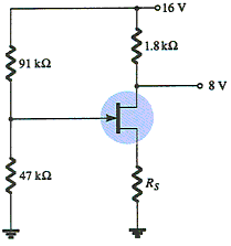
18. For R2 smaller than _____ kΩ the voltage VD is equal to VDD = 16 V.
- A) 3.75
- B) 5
- C) 12.0
- D) 24
19. _____ must be considered in the total design process.
- A) Dc conditions
- B) Level of amplification
- C) Signal strength
- D) All of the above
20. In a JFET, the level of _____ is limited to values between 0 V and –VP.
- A) VSQ
- B) VDGQ
- C) VDSQ
- D) VGSQ
21. The level of VDS is typically between _____ % and _____ % of VDD.
- A) 0, 100
- B) 10, 90
- C) 25, 75
- D) None of the above
22. In a universal JFET bias curve, the vertical scale labeled m is used to find the solution to the _____ configuration.
- A) fixed-bias
- B) self-bias
- C) voltage-divider
- D) None of the above
23. In a universal JFET bias curve, the vertical scale labeled M is used for finding the solution to the _____ configuration.
- A) fixed-bias
- B) self-bias
- C) voltage-divider
- D) None of the above
24. In a universal JFET bias curve, the horizontal axis is _____.
25. In p-channel FETs, the level of VGS is _____ while the level of VDS is _____.
- A) negative, negative
- B) positive, positive
- C) negative, positive
- D) positive, negative
Back to Homepage
Note: Check your works. DC Biasing – FETs - MCQs Answers






0 comments: Post Yours! Read Comment Policy ▼
PLEASE NOTE:
I have Zero Tolerance to Spam. It will be deleted immediately upon review.
Post a Comment